


Intel Off Campus Hiring For Silicon Packaging Design Engineer | Bangalore
Intel Off Campus 2026: Silicon Packaging Design Engineer Hiring in Bangalore
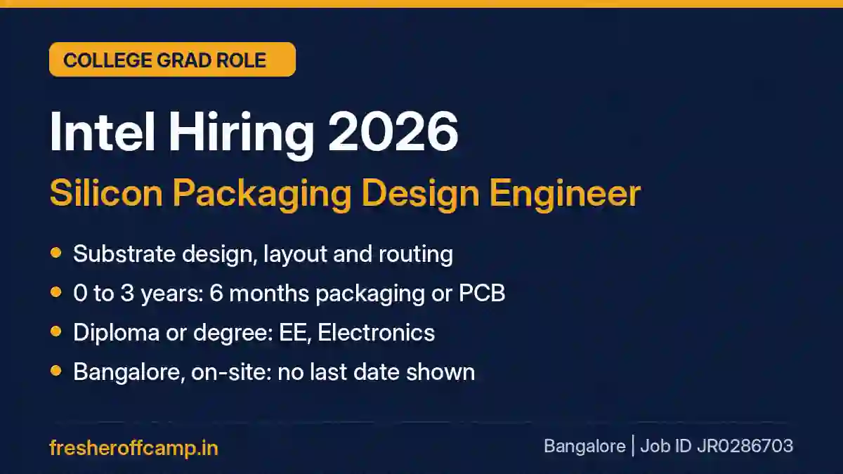
Intel Silicon Packaging Design Engineer (job ID JR0286703) is an early-career opening at Intel in Bangalore. It is tagged College Grad with 0 to 3 years of experience, but you need at least six months of semiconductor work in silicon packaging or PCB design. Diploma or degree holders in electrical or electronics engineering can apply on Intel Workday. No last date is shown.
This guide explains what an Intel Silicon Packaging Design Engineer does, who can apply, the skills to show, a reported salary range, the likely interview steps and how to apply.
Last updated: 16 November 2026
Quick Overview
| Detail | Information |
|---|---|
| Company | Intel Technology India |
| Role | Silicon Packaging Design Engineer |
| Job ID | JR0286703 |
| Location | Bangalore, Karnataka |
| Hiring type | College Grad |
| Experience | 0 to 3 years, with 6+ months in packaging or PCB design |
| Qualification | Diploma in Electronic or Electrical Engineering or related; a related degree also fits |
| Batch | Not mentioned |
| Salary | Not disclosed (see the salary section) |
| Work mode | On-site, Shift 1 (India) |
| Employment type | Full time |
| Interview rounds | Not shown in the listing |
| Last date | Not shown |
Important: this is not a pure fresher role. Students with no internship or job in packaging or PCB design do not meet the minimum experience line.
Read Also:-
Qualcomm Off Campus 2026 Hiring Fresher For Associate Engineer / Software Engineer | Hyderabad / Chennai / Bangalore:- CLICK HERE
American Express Off Campus 2026 Hiring Fresher For TCPS Analyst | Gurugram:- CLICK HERE
Table of Contents
- About the role
- Job responsibilities
- Eligibility criteria
- Skills required
- Salary for freshers
- Selection process
- Interview tips
- How to apply
- Important dates
- Common mistakes
- FAQs
- Final Words
About Intel and the Intel Silicon Packaging Design Engineer Role
Intel is an American semiconductor company that designs and makes processors for laptops, desktops and data centres. Its Bangalore teams work on chip design, validation, software and packaging.
A processor die cannot be soldered straight onto a motherboard. It sits on a package substrate, a small multi-layer board that routes thousands of tiny bumps on the die out to the larger balls or pins that meet the motherboard. It also carries power to the chip.
An Intel Silicon Packaging Design Engineer draws that substrate. The listing describes the work as driving substrate designs from concept through tapeout, doing the physical layout and routing, and running fit and routing studies that balance performance and cost. It sits in the Intel Data Center Group, according to the Workday page.
Intel Silicon Packaging Design Engineer Job Responsibilities
According to the official listing, the person in this role will:
- Drive substrate designs from the first concept through tapeout
- Do the physical layout and routing of package designs to meet requirements
- Run substrate fit and routing studies to balance design, performance and cost
- Work with silicon and hardware teams on silicon-package-board performance and pinout
- Define and apply substrate design rules
- Join internal and external design reviews and fix design rule violations (DRCs)
- Keep design documents in the product lifecycle management (PLM) system
- Find ways to improve design for manufacturing (DFM) and quality
Intel Silicon Packaging Design Engineer Eligibility Criteria
| Criteria | Official detail |
|---|---|
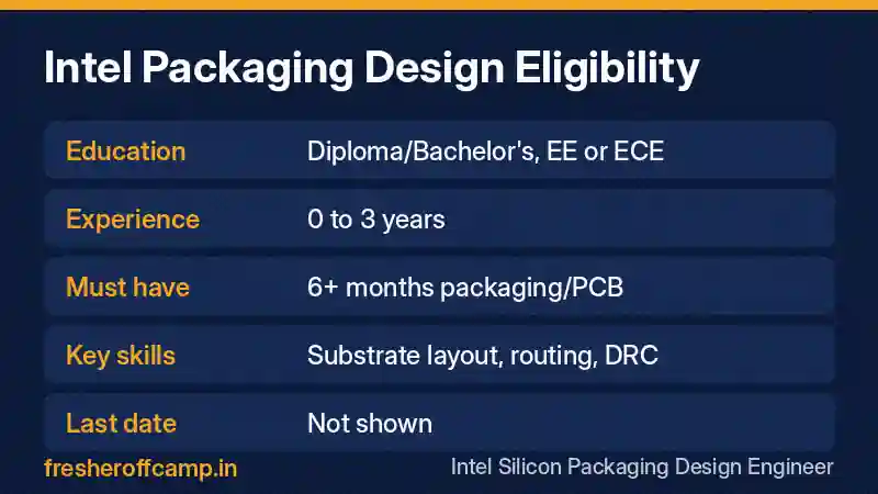
| Education | Diploma in Electronic or Electrical Engineering or a related field (minimum line) |
| Degree | A copy of the listing on a job board also asks for a Bachelor’s degree; BE or BTech in ECE or EEE fits both |
| Experience | 0 to 3 years, College Grad tag |
| Must have | At least 6 months of semiconductor work in silicon packaging or PCB design |
| Skill level | Novice to intermediate in substrate layout and routing |
| Batch and marks | Not mentioned in the listing |
The six-month experience line is the main filter for the Intel Silicon Packaging Design Engineer job. An internship in PCB layout, a job at a PCB design service firm or a stint in an OSAT (assembly and test) company can count, as long as it involved real layout or routing work. Put the duration and the tool you used right at the top of your resume.
Who should not apply
- Students with no packaging or PCB design work at all
- Software or IT freshers without hardware layout exposure
- People looking for a remote or hybrid job, since the listing says on-site
- Candidates with more than 3 years of experience
Skills Required for Intel Silicon Packaging Design Engineer
Technical skills
| Skill | Priority | What to practise |
|---|---|---|
| Substrate or PCB layout | High | Place parts, route traces, plan layer stack-up |
| DRC and design rules | High | Read a rule deck and fix spacing and width errors |
| I/O and power delivery basics | High | Impedance, return paths, decoupling and power planes |
| Package interconnect | Medium | Flip-chip bumps, vias, BGA balls and their pitch |
| E-CAD tools | Medium | Cadence Allegro, Siemens Xpedition or similar |
| DFM and quality | Medium | Why some layouts are hard to build and cost more |
Soft skills
The listing asks for clear technical communication, cross-functional teamwork, a disciplined way of working and the habit of looking for design improvements.
Intel Silicon Packaging Design Engineer Salary for Freshers
Intel has not disclosed the salary for this Intel Silicon Packaging Design Engineer opening. AmbitionBox shows Intel Design Engineer pay for freshers at about 8 to 26 LPA, based on 33 self-reported fresher salaries. Its Packaging Engineer page has only one entry, so we do not use it.
Treat these numbers as reported estimates, not an offer.
| What changes the pay | How it affects the offer |
|---|---|
| Education | Degree holders may get a higher band than diploma holders |
| Relevant experience | 6 months versus 2 to 3 years of layout work changes the offer |
| Tool skills | Hands-on Allegro or Xpedition work can help in negotiation |
| Benefits | Intel lists benefits on its careers site; the listing itself does not give a figure |
Compare packages in our fresher salary in top companies guide.
Intel Silicon Packaging Design Engineer Selection Process (Expected)
The listing does not name the interview rounds for the Intel Silicon Packaging Design Engineer role. Hardware design roles at large chip companies often follow a pattern like this:
- Resume shortlisting: your packaging or PCB experience and tools are checked.
- Technical interview 1: layout basics, stack-up, DRC, vias and routing rules.
- Technical interview 2: signal and power integrity basics, and a walk-through of a design you did.
- Manager or HR round: on-site readiness, joining date and teamwork questions.
Treat these steps as a guide and follow only what Intel shares by email or in your Workday account.
Intel Silicon Packaging Design Engineer Interview Tips and Sample Answers
Q1. What does a package substrate do?
Sample answer: “It connects the fine-pitch bumps on the die to the larger balls on the board. Inside its layers it routes signals, carries power and ground, and spreads the connections out so the board can handle them.”
Q2. How do you fix a spacing DRC error in a dense area?
Sample answer: “First I check whether the rule is a hard manufacturing limit or a preferred value. Then I try rerouting the trace, moving it to another layer through a via, or adjusting nearby parts. I avoid shrinking the clearance below the rule just to make the error disappear.”
Q3. Why is power delivery important in a package?
Sample answer: “A modern chip draws large and fast-changing currents. If the power planes and decoupling are weak, voltage drops and noise appear, which can make the chip fail at speed. Good planes and enough vias keep the supply stable.”
For HR answers and a self-introduction template, use our free Interview Kit for freshers.
How to Apply for Intel Silicon Packaging Design Engineer 2026
Applications for the Intel Silicon Packaging Design Engineer job go through Intel’s Workday careers portal. Click the button below to open the official listing.
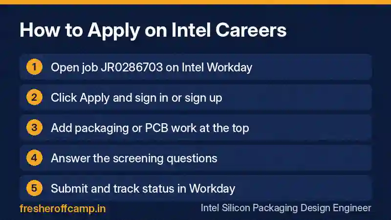
- Click the Apply Link to open job JR0286703 on Intel Workday.
- Click Apply and sign in or create a candidate account.
- Fill in your education and add your packaging or PCB experience with dates.
- Upload a one-page resume that names the E-CAD tools you used.
- Answer the screening questions, review and submit.
Fraud warning: the Intel listing says candidates should never be asked to pay recruitment, medical or other fees. Apply only through the official Intel careers site.
Want other Intel openings? See our Intel internship and freshers hiring guide. Getting no replies? Read why freshers get no interview calls, use our free job hunt resources for guides and toolkits, and check the Fresheroffcamp.in homepage for more openings.
Intel Silicon Packaging Design Engineer Important Dates
| Event | Date or status |
|---|---|
| Posted date | Not shown on the listing we could read |
| Last date | Not shown |
| Interview dates | Shared by Intel after shortlisting |
Common Mistakes Freshers Make
- Applying with no packaging or PCB work and hoping the College Grad tag is enough
- Writing vague lines like worked on PCB without tools, layers or duration
- Skipping power delivery and signal basics while preparing
- Waiting too long because no last date is shown
- Paying anyone who promises an Intel job
Frequently Asked Questions
What is the last date to apply for Intel Silicon Packaging Design Engineer?
The listing does not show a last date. Openings like this can close without notice, so apply soon.
Who can apply for the Intel Silicon Packaging Design Engineer job?
Candidates with a diploma or degree in electrical, electronics or a related field, 0 to 3 years of experience and at least six months of packaging or PCB design work.
Can freshers apply for Intel Silicon Packaging Design Engineer?
Yes, if they have at least six months of semiconductor work in packaging or PCB design, for example through an internship. Freshers without that experience do not meet the minimum line.
Can BTech ECE or EEE graduates apply for this Intel job?
Yes. A BE or BTech in ECE or EEE is a related qualification, and the experience line still applies.
What is the Intel Silicon Packaging Design Engineer salary?
Intel has not disclosed it. AmbitionBox shows Intel Design Engineer fresher pay of about 8 to 26 LPA, which is only a reported estimate.
Is the Intel Silicon Packaging Design Engineer job work from home?
No. The listing says the role is on-site in Bangalore.
What is the job ID for Intel Silicon Packaging Design Engineer in Bangalore?
The job ID is JR0286703.
What is the Intel recruitment process for this role?
The listing does not say. Expect resume shortlisting, one or two technical interviews and a manager or HR round.
Does Intel charge any fee for jobs?
No. The listing says candidates should never be asked to pay any recruitment or other fee.
Where can I find official Intel job openings in India?
On Intel’s Workday careers site. Search for India or Bangalore to see current roles.
Final Words on Intel Silicon Packaging Design Engineer
The Intel Silicon Packaging Design Engineer role suits ECE and EEE candidates who already have some hands-on packaging or PCB layout work and want to grow in chip packaging. Polish your layout examples, revise power delivery and DRC basics, and apply through the official link above.
Disclaimer: Fresheroffcamp.in is not linked to Intel. Hiring status, eligibility, salary and the selection process can change. Confirm every detail on the official listing.



Leave a Reply